


2022-07-16
This article is excerpted from "ijiwei APP".
Overview: The growth of digital economy along with its intelligent applications drives the explosive growth of the semiconductor industry in all aspects, and has become a key force to stimulate economic growth. Due to the close ties between semiconductor industry and EDA field, the applications of EDA tools are rapidly extending. EDA field is now facing unprecedentedly complext systematic chip design and manufacturing processes. As an EDA company with high-end market competitiveness, Phlexing dedicates to the field of chip's physical parameters and has independently developed EDA tools repository, including parasitic parameter extraction, power integrity, electromigration, reliability and multi-physical domain, etc., Phlexing is committed to addressing growing challenges faced by both IC design and fabrication partners.
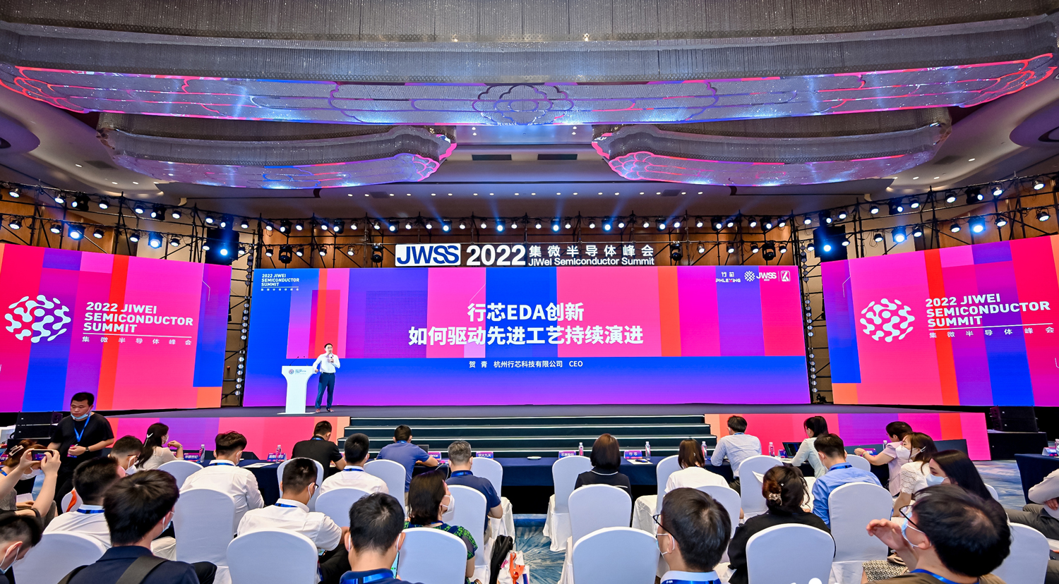
According to ijiwei news, on July 15, the "2022 6th Jiwei Semiconductor Summit-EDA IP Summit" was held in Xiamen. At the meeting, Dr. Qing He, Chairman and General Manager of Phlexing Technology Co., Ltd., analyzed the current technical challenges faced by EDA tools for advanced technologies, and presented Phlexing's views on how EDA innovation drives the continuous evolution of semiconductor industry.
Technical bottlenecks of EDA
EDA tools have played a key role in advancing/propelling semiconductor technology since chip design entered the age of automation, and have played a pivotal role not only in designing, but also in validation and manufacturing. With digital transformation in a global scale, the market demand for chips is more diversified, from simple consideration/metrics of power consumption, performance, area and other general performance improvement, to conclusive specifications in application scenarios, software, algorithms, hardware and other requirements. The change from two-dimensional world to three-dimensional world renders current chip design, especially EDA tools, both a great challenge and a great opportunity. At the EDA IP Summit, Qing He analyzed difficulties encountered in the fast-innovating EDA industry.
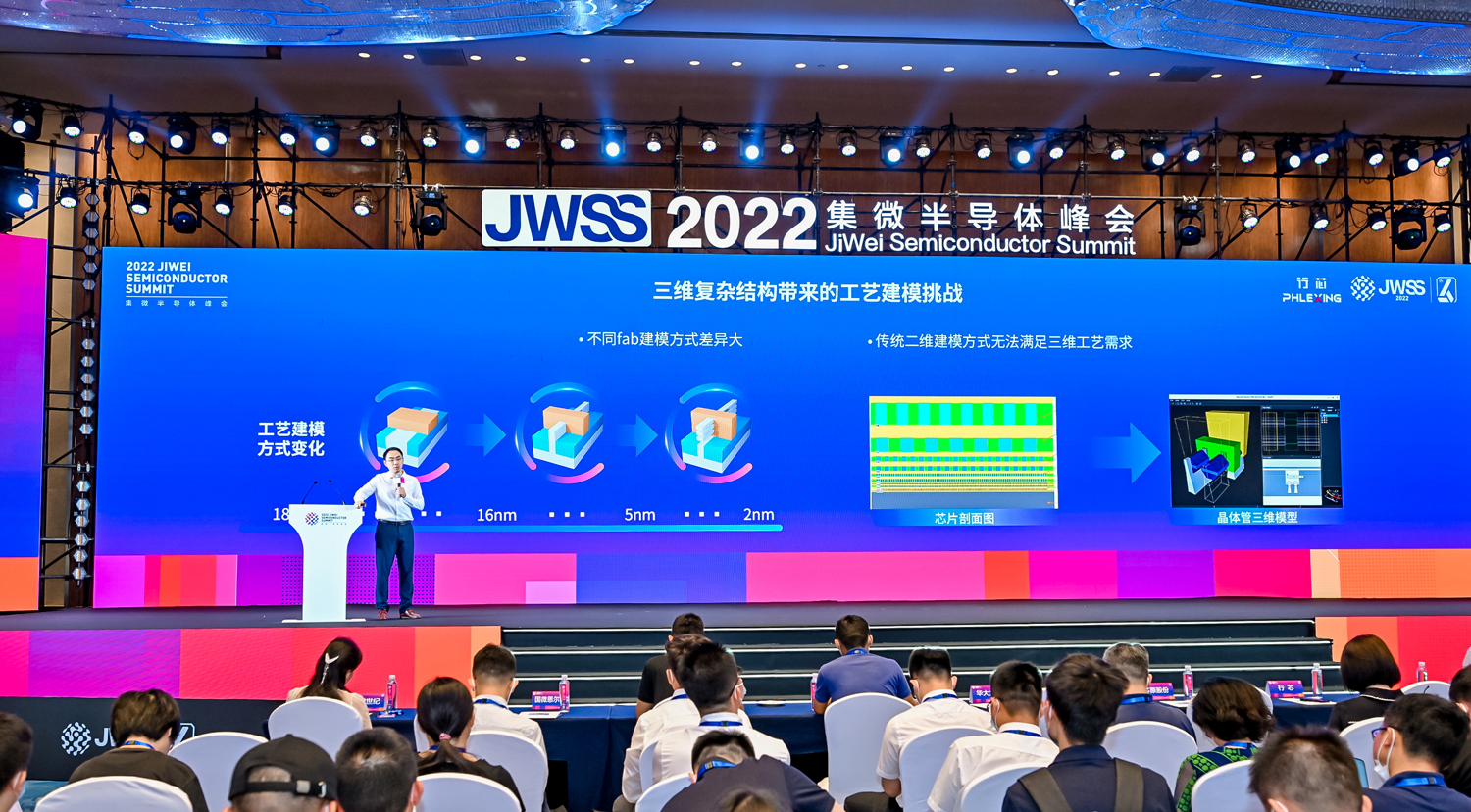
First, Qing He pointed out that, with the evolution of advanced technology from 2D to 3D at the micro scale of devices and the macro scale of systems, the traditional 2D modeling method failed to meet complex requirements of 3D technology This is the first and major challenge brought by the 3D complex model. Second, as the fabrication process nodes continue to advance towards smaller, such as 5nm and 3nm, units, transistor miniaturization brings arrays of complex processing side effects; EDA tools face multiple challenges including multiple exposure, process jitter, multiple dielectric layers and etch loads. It is difficult to push Moore's Law forward. Then, "in addition to the micro-scale challenges posed by pure processes, a mix of processes and architectures coupled with electrical, thermal, electromagnetic, and mechanical effects must be included in three-dimensional integration. This is never considered in traditional chip design." Qing He said.
Qing He used a metaphor of intenser traffic running on more complex roads for the situation faced by integrated circuits while evolving. He stated that the evolution of integrated circuits has been marked by increasingly larger scale, resulting in increasingly insufficient computing capability. As the number of transistors and RC parameters continues to increase, chip design cycles extend, simulations fail in certain aspects, and IT demand peaks. These all put a huge burden on IC design companies. When this pressure is transferred/passed to EDA tools, our industry needs overcome problems including strong tool dependence, computational stability and consistency, precision relaxation control, AI speed improvement and prediction, and new computing architectures.
Innovation in precision, efficiency and capacity
In Qing's opinion, the ultimate challenge presented by chip's power consumption, performance and cost is not only a scientific or engineering problem, but even an issue of Art. "Innovations in EDA should return to the nature of physics." Qing He said that Phlexing has, in a high-precision way, pioneered a 2D/3D unified modeling methodology to target essential, physical level problems such as precision, efficiency and capacity in chip design that supports large-capacity computing at all levels. Then, Qing He presented one of Phlexing's independently developed EDA tools as an example to share some innovative highlights that Phlexing has lit while coping with power consumption, performance and cost.
According to Qing He, Phlexing has developed its own large-capacity computing platform, launched high accuracy full-chip parasitic extraction solution GloryEX full-chip power and reliability Signoff solution GloryBolt,and multi-physics solver for 3D IC chips PhyBolt. GloryEX provides high accuracy RC parasitic parameter extraction solutions with Signoff accuracy, supports high-precision simulation of 3D complex structures and supports modeling of various processes including back end, middle end and advanced process. Given that customers tend to demand for larger design capacity that exceeds the existing computing capability, Phlexing uses elastic computing architecture to support super capacity computing. Qing He said that Phlexing's EDA tools revolutionize through fundamental computing architecture and support large-scale computing of millions of analog transistors, hundreds of millions of digital circuits and billions of computing scale, These tools build up the Glory large-capacity platform, with innovations instilled into each product to solve problems involved in designing devices, IP, SoC and IC systems.
Fuel synergy between design and manufacturing, and drive continuous processing evolution
Finally, in a broad view, Qing He expressed his views on the EDA's role in driving the continuous evolution of advanced processes.. He said that, in the post-Moore era, design process in EDA, lacks relevance/connections to particular needs of system-level hardware and software.. In the process of EDA evolution, from point tool, to platform tool, to the full-flow process tool, and then to the intelligent full-flow process with infinite computing capability, there is only one goal: to shorten the gaps between different processes. This goal is achieved through continuous evolution of products matrix and the deep collaboration between design and manufacturing. EDA tools, powered with intelligence running on a high capacity platform, are strong enough to provide, full-flow process solutions integrated with infinite computing capability. "As EDA tool matrix continues to evolve, Phlexing is committed to exploring technological innovations with regard to precision, efficiency, scale and other aspects. Through its services with top IC design companies, Phlexing, honors seamless collaboration between design and manufacturing and contributes to the continuous evolution of advanced EDA technology."
EDA/IP Empowering China's Chips Roundtable Forum
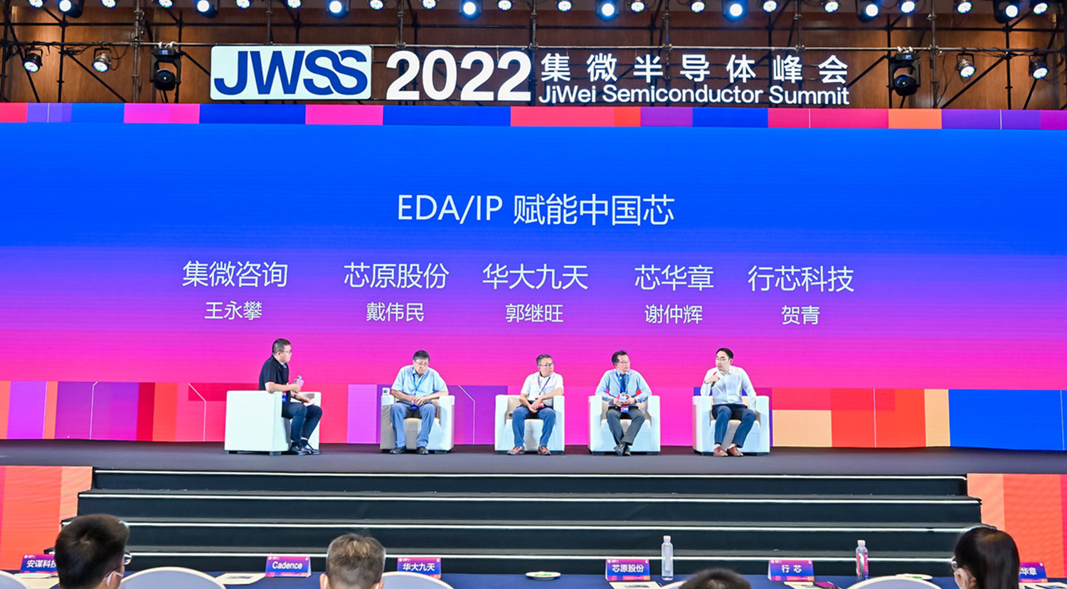
At the EDA/IP Empowering China's Chips Round-table Forum, Qing He emphasized on the spirit of cooperation on the hot topic of how EDA tools work with design and manufacturing. He pointed out the challenge of deeper cooperation between different sectors, in the IC industry. The cooperation should not only generate specific features but also come with high efficiency and comparative advantages. If EDA just plays the role of point optimization at every single dot of simulation, it is just a drop in the ocean. In the long run, it is necessary to build a good industrial 'ecosystem' to infuse so many droplets together to help chip design and fibrication. "From Fabrication's point of view, the quality of EDA tools is rather uninfulential, but how EDA companies position themselves as suppliers or partners is critical; From the perspective of chip design, ensuring the quality of final chip is a major concern. Between EDA and design, the closer integration, the higher possibility of success. This tie needs to connect all the underlying data links, and build a trust mechanism. Such deep collaboration will certainly shine with its own features and top speed." Qing He finally said.
 Zhejiang public network security 33010802011331